研究目的
Investigating the optical and electrical properties of films and field-effect transistors (FETs) based on pure MEH-PPV, neat CsPbBr3 nanocrystals (NCs), and MEH-PPV:CsPbBr3 NCs composites with different contents of CsPbBr3 NCs.
研究成果
The study demonstrated that MEH-PPV:CsPbBr3 NCs composite films exhibit promising optical and electrical properties for applications in nanotechnology LEDs, FETs, and LE-FETs. The superlinearity of EL intensity with increasing CsPbBr3 NCs concentration and the efficient energy transfer between NCs and the polymer matrix were highlighted as key findings.
研究不足
The study focuses on the optical and electrical properties at specific temperatures and excitation powers. The effects of varying other parameters such as film thickness, NC size, and different polymer matrices were not explored.
1:Experimental Design and Method Selection:
The study involved the preparation of polymer-perovskite composite films and the fabrication of FETs based on these films. The films were characterized using absorbance, atomic-force microscope, and current-voltage characteristics techniques. PL and EL intensities and spectra were measured at various levels of optical and electrical excitation power.
2:Sample Selection and Data Sources:
Samples included pure MEH-PPV, neat CsPbBr3 NCs, and MEH-PPV:CsPbBr3 NCs composites with different contents of CsPbBr3 NCs. Data were collected from absorbance spectra, AFM profiles, PL and EL measurements, and I-V characteristics of FETs.
3:List of Experimental Equipment and Materials:
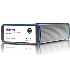
Equipment used included an Atomic Force Microscopy (AFM) - SOLVER P47-PRO NT-MDT, Cary-50 (Varian) spectrometer, high-sensitivity fiber optic spectrometer with ultra-light scattering 'AVANTES' – AvaSpec-ULSi2048L-USB2 OEM, and a photomultiplier for time-resolved intensity measurements.
4:Experimental Procedures and Operational Workflow:
The films were prepared by drop-casting solutions onto substrates, followed by drying and heating. FET structures were fabricated by drop-casting solutions onto doped silicon substrates with thermally grown SiO2 and evaporated electrodes. Measurements were conducted at various temperatures and excitation powers.
5:Data Analysis Methods:
The hole mobility was calculated using equations for saturation and weak electric field regimes of output I-Vs. The temperature dependence of hole mobility was analyzed to understand the transport mechanism.
独家科研数据包����,助您复现前沿成果���,加速创新突破
获取完整内容